Table of Contents
The following lists show important hardware details of all supported hardware platforms of this VisualApplets version. For a detailed list, please check the data sheet of the individual product.
| Resource | imaFlex CXP-12 Quad | imaFlex CXP-12 Penta | imaFlex 2 Dual 100 | ||||||||||
|---|---|---|---|---|---|---|---|---|---|---|---|---|---|
| Vision Processor | Xilinx UltraScale+ XCKU3P-FFVD900-1-E | Xilinx UltraScale+ XCKU3P-FFVB676-1-E | Xilinx UltraScale+ XCKU15P-FFVE1517-1-E | ||||||||||
| LUT | 160679 | 161049 | 447992 | ||||||||||
| Flip-Flop | 323224 | 323216 | 895984 | ||||||||||
| Block RAM (18k) | 720 | 720 | 1776 | ||||||||||
| URAM Blocks (288k) | 48 | 48 | 128 | ||||||||||
| Embedded Arithmetic Logic Unit (DSP48) | 1368 | 1368 | 1800 | ||||||||||
| RAM size | 3 x 512 MiB DDR4 | 5 x 512 MiB DDR4 | 2 @ 5 x 1024 MiB DDR4 | ||||||||||
| RAM Data Width | 384 Bit | 640 Bit | 640 Bit | ||||||||||
| RAM Bandwidth total (shared) | 14.4 GB/ |
24.0 GB/s |
2 @ 24.0 GB/s |
||||||||||
| Base Design Clock (default) | 312.5 MHz |
312.5 MHz |
391.5 MHz |
||||||||||
| Base Design Clock (maximal) | 400.0 MHz | 400.0 MHz | 420.0 MHz | ||||||||||
| Host Interface | PCIe x 8 Gen 3 (Direct Memory Access) | PCIe x 8 Gen 3 (Direct Memory Access) | PCIe x 16 Gen 3 (Direct Memory Access) | ||||||||||
| Host Interface (PCIe x 8 Gen 3) Bandwidth (theor.) | 8000 MB/s | 8000 MB/s | 16000 MB/s | ||||||||||
| Host Interface (PCIe x 8 Gen 3) Bandwidth (typ./max.) | 7200 MB/s sustainable data bandwidth | 7200 MB/s sustainable data bandwidth | 13000 MB/s sustainable data bandwidth |
||||||||||
|
|||||||||||||
Table 68. Hardware Configuration imaFlex platforms
| Resource | mE5 marathon VCX-QP | mE5 marathon VCL | mE5 marathon VCLx | ||||
|---|---|---|---|---|---|---|---|
| Vision Processor | Xilinx Kintex7 XC7K160T - 2FFG676C FPGA | Xilinx Kintex7 XC7K160T - 1FBG676C FPGA | Xilinx Kintex7 XC7K410T - 1FBG676C FPGA | ||||
| LUT | 101400 | 101400 | 254200 | ||||
| Flip-Flop | 202800 | 202800 | 508400 | ||||
| Block RAM (18k) | 650 | 650 | 1590 | ||||
| Embedded Arithmetic Logic Unit (DSP48) | 600 | 600 | 1540 | ||||
| RAM size | 4 x 512MiB DDR3 | 4 x 512MiB DDR3 | 4 x 512MiB DDR3 | ||||
| RAM Data Width | 512 Bit | 256 Bit | 256 Bit | ||||
| RAM Bandwidth total (shared) | 12.8 GB/s |
6.4 GB/s |
6.4 GB/s |
||||
| Base Design Clock (default) | 125MHz | 125MHz | 125MHz | ||||
| Base Design Clock (maximal) | 312.5 MHz |
312.5 MHz |
312.5 MHz |
||||
| Host Interface | PCIe x 4 Gen 2 (Direct Memory Access) | PCIe x 4 Gen 2 (Direct Memory Access) | PCIe x 4 Gen 2 (Direct Memory Access) | ||||
| Host Interface (PCIe x 4 Gen 2) Bandwidth (theor.) | 1x2000 MB/s | 1x2000 MB/s | 1x2000 MB/s | ||||
| Host Interface (PCIe x 4 Gen 2) Bandwidth (typ./max.) | Up 1800 MB/s sustainable data bandwidth | Up to 1800 MB/s sustainable data bandwidth | Up to 1800 MB/s sustainable data bandwidth | ||||
|
|
|||||||
Table 69. Hardware Configuration microEnable 5 marathon
Device resources are limited on each hardware platform. The lists below show the available resources for all supported platforms. Operators consume device resources, and most resource instances can be used only once. There are some exceptions to this rule, e.g., the GPI operator. In these cases, resource consumption is documented in the operator reference documentation.
Device resources are allocated either
-
automatically,
-
using operator parameters, or
-
in the Resources dialog.
See 'Allocation of Device Resources' for more information.
| Resource | imaFlex 2 Dual 100 | ||||||||
|---|---|---|---|---|---|---|---|---|---|
| Port[0] CoF Lane |
4 | ||||||||
| Port[1] CoF Lane |
4 | ||||||||
| Port[0] CoF RX Trigger Lane |
4 | ||||||||
| Port[1] CoF RX Trigger Lane |
4 | ||||||||
| Port[0] CoF TX Trigger Lane |
4 | ||||||||
| Port[1] CoF TX Trigger Lane |
4 | ||||||||
| Port[0] CoF Status Lane |
4 | ||||||||
| Port[1] CoF Status Lane |
4 | ||||||||
| Port[0] DF RX Data Lane |
4 | ||||||||
| Port[1] DF RX Data Lane |
4 | ||||||||
| Port[0] DF RX Meta Lane |
4 | ||||||||
| Port[1] DF RX Meta Lane |
4 | ||||||||
| Port[0] DF TX Data Lane |
4 | ||||||||
| Port[1] DF TX Data Lane |
4 | ||||||||
| Port[0] DF TX Meta Lane |
4 | ||||||||
| Port[1] DF TX Meta Lane |
4 | ||||||||
| Port[0] DF Green LED Lane |
4 | ||||||||
| Port[0] DF Red LED Lane |
4 | ||||||||
| Port[1] DF Green LED |
1 | ||||||||
| Port[1] DF Red LED |
1 | ||||||||
| DmaToHostPort |
5 | ||||||||
| DmaFromHostPort |
1 | ||||||||
| GPI |
16 | ||||||||
| GPO |
16 | ||||||||
| EventPort |
31 | ||||||||
| EventID |
64 | ||||||||
| User LED |
6 | ||||||||
| ImageChannel |
1024 | ||||||||
| RAM |
2 @ from 1 x 5 GiB to 8 x 625 MiB | ||||||||
|
|||||||||
Table 70. List of Device Resources imaFlex 2 Dual 100
| Resource | imaFlex CXP-12 Quad | imaFlex CXP-12 Penta | ||||||||||||
|---|---|---|---|---|---|---|---|---|---|---|---|---|---|---|
| Camera Port | 4 | 5 | ||||||||||||
| CxpStatusPort | 4 | 5 | ||||||||||||
| CxpRxTriggerPort | 4 | 5 | ||||||||||||
| CxpTxTriggerPort | 4 | 5 | ||||||||||||
| DMA | 4 | 5 | ||||||||||||
| DmaFromHostPort | 1 | 1 | ||||||||||||
| GPO |
10 OUT | 12 OUT | ||||||||||||
| GPI |
12 IN | 12 IN | ||||||||||||
| LED Ports |
6 | 6 | ||||||||||||
| SignalChannel |
4000 | 4000 | ||||||||||||
| EventPort |
32 | 32 | ||||||||||||
| EventID |
64 | 64 | ||||||||||||
| ImageChannel |
1024 | 1024 | ||||||||||||
RAM |
from 1 x 1.5 GiB to 8 x 192 MiB | from 1 x 2.5 GiB to 8 x 320 MiB | ||||||||||||
|
||||||||||||||
Table 71. List of Device Resources imaFlex CXP-12 Quad and imaFlex CXP-12 Penta
Table 72. List of Device Resources microEnable 5 marathon
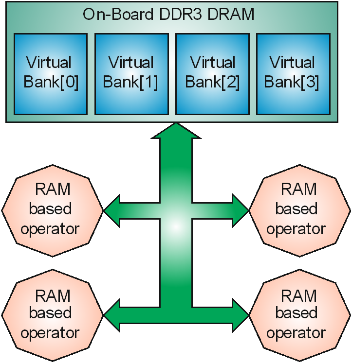
The imaFlex 2 Dual 100 platform contains two separate physical RAM banks, each with a capacity of 5 GiB. These physical banks are divided into non-overlapping memory regions as needed, based on the number of RAM-based VisualApplets operators used in an applet. Within VisualApplets, these regions appear as virtual RAM banks. When an operator requires RAM, it reserves a virtual RAM bank, which corresponds to a dedicated, non-overlapping region within the physical RAM.
On the imaFlex 2 Dual 100 platform, you can define up to 8 non-overlapping memory regions per physical RAM bank, which means a total of 16 regions across both RAM interfaces. If only one RAM operator is assigned to a physical interface, it has access to the entire 5 GiB capacity of that interface. When multiple operators share the same physical interface, the available memory is divided proportionally among them. For example, if 8 operators are assigned to the same interface, each operator receives 1/8 of the 5 GiB memory, resulting in approximately 0.625 GiB per operator.
The RAM bandwidth on the imaFlex 2 Dual 100 is shared evenly among all operators connected to the same physical interface; it is not exclusive to any single operator.
-
If a design uses all 8 RAM resources on one interface, each RAM-based operator will receive approximately 1/8 of the total interface bandwidth, adjusted by the operator’s efficiency factor.
-
If only one RAM-based operator is used, it can utilize the full maximum bandwidth of that interface.
-
If two operators share the same interface, each will receive half of the total bandwidth, and so on.
The 2 physical RAM interfaces of the platform are mapped to 16 virtual RAM ports in VisualApplets. The first RAM interface is mapped to the RAM resource index 0 to 7, and the second is mapped to the RAM resource index 8 to 15.
RAM ports that are not allocated (and therefore not used) always receive 0% of the memory capacity. This means the total available memory is divided only among the operators that are actively using the RAM ports.
-
If only 1 port is used: That port receives 100% of the available memory.
-
If 2 ports are used: Each port receives 50% of the available memory.
-
If 3 ports are used: The port with the lowest resource ID receives 50%, and the other 2 ports each receive 25%.
-
If 4 ports are used: All 4 ports receive 25% each.
-
If 5 ports are used: The first 3 ports (with the lowest resource IDs) each receive 25%, and the remaining 2 ports each receive 12.5%.
-
If 6 ports are used: The 2 ports with the lowest resource IDs each receive 25%, and the other 4 ports each receive 12.5%.
-
If 7 ports are used: The port with the lowest resource ID receives 25%, and the other 6 ports each receive 12.5%.
-
If 8 ports are used: All ports receive 12.5% each.
![[Note]](../common/images/admon/note.png) |
Asymmetric Memory Allocation |
|---|---|
|
Ports with the lowest RAM index within the same physical bank receive a larger allocation in case of asymmetric size partitioning. For example, if 3 RAM ports are used (0, 1, and 2), port 0 receives 50% of the RAM size, while ports 1 and 2 each receive 25%. The same applies if the ports are 8, 9, and 10, as they map to the second RAM interface but still belong to the same physical RAM bank. |
The RAM indexes do not need to be contiguous; their absolute order determines the allocation. The RAM index is a virtual identifier and does not affect FPGA resource usage, even if there are gaps in the sequence. For example, if 3 RAM ports are used (1, 5, and 7): Port 1 receives 50% of the RAM size, and ports 5 and 7 each receive 25%.
There is no advantage or disadvantage in how RAM indexes are allocated when all resources map to the same physical bank. You can use the automatic allocation provided by VisualApplets or adjust it manually if a specific design operator requires more RAM than others.
|
Independent RAM Interfaces |
|---|---|
|
Both physical RAM interfaces are completely independent. For example, if two operators are used and one is assigned to the first RAM interface while the other is assigned to the second, each operator can utilize the full maximum RAM size of its respective interface. |
The shared memory controller uses a Round-robin algorithm to distribute bandwidth evenly across all allocated ports within a physical RAM interface. This algorithm is based on a credit-based arbitration scheme. When a port becomes active, it remains active for a set number of credit clock cycles, as long as it continues to provide new RAM jobs. If an active port has no more jobs, it is deactivated, and the activation token moves to the next port with pending requests. This ensures that bandwidth is never wasted on idle ports.
The credit values are programmed by the firmware during applet synthesis, based on the number of RAM operators used. They can't be changed at runtime or through the Framegrabber SDK. Users have no access to credit configuration.
While a port is active, it has 100% of the memory controller bandwidth. If all 8 ports in a physical bank are active evenly, each port receives approximately 1/8 of the total bandwidth over time. In other cases, the actual average bandwidth depends on the load of each port.
The physical RAM interfaces are completely independent. Assigning RAM-based operators to different interfaces maximizes bandwidth efficiency. Bandwidth is shared only among operators that are connected to the same physical RAM interface.
The imaFlex 2 Dual 100 provides 2 independent physical RAM interfaces. Each interface has its exclusive bandwidth and memory size. When maximal bandwidth and size is targeted in a design, place RAM-based operators evenly between both RAM interfaces. Ports 0 to 7 are mapped to the first RAM interface, and ports 8 to 15 are mapped to the second.
The platforms imaFlex CXP-12 Quad and imaFlex CXP-12 Penta are assembled with only one physical RAM bank (the size of which is platform-specific). This single physical bank is dynamically formatted into non-overlapping regions depending on the amount of used RAM-based VisualApplets operators inside the applet. Those regions are represented inside VisualApplets as virtual RAM banks. When an operator reserves a RAM resource, it is using a virtual RAM bank which maps to an exclusive non-overlapping memory region inside the physical RAM. Up to 8 non-overlapping regions can be defined on the imaFlex platforms. When only 1 RAM operator is used, the operator gets the complete RAM size of the platform. The allocated size for each additional operator reduces the operator’s owned size proportionally to the operator’s amount docking on the same physical interface. If 8 operators are used, each operator will allocated 1/8 of the platform memory size.
The RAM bandwidth, however, is shared between all RAM-based operators in a design. When a design utilizes all 8 RAM resources, each of the 8 RAM-based operators can have up to 1/8 GB/s exclusive bandwidth, minus the efficiency factor of that particular operator. When only one RAM-based operator is used in the design, this operator gets the total bandwidth of the platform. When 2 operators are used, each of the two operators gets half the total bandwidth, etc.
Not allocated and thus not used RAM ports get always 0% of the memory size.
-
1 port is used: the used port gets 100%.
-
2 ports are used: both used ports get 50%.
-
3 ports are used: the port with the lowest resource ID number will get 50%, the other 2 used ports get 25%.
-
4 ports are used: all 4 ports get 25%.
-
5 ports are used: 3 ports with the lowest resource ID number will get 25%. The last 2 ports will get 12.5%.
-
6 ports are used: 2 ports with the lowest resource ID number will get 25%. The other 4 ports will get 12.5%.
-
7 ports are used: the port with the lowest resource ID number will get 25%. The other 6 ports will get 12.5%.
-
8 ports are used: all ports get 12.5%.
|
|
|
Ports with the lower RAM index will get larger allocation in case of asymmetric size partitioning. For example 3 RAM ports are used: 0, 1, 2. The port 0 gets 50% RAM size allocation. The ports 1 and 2 get both 25% each. The RAM indexes do not need to be contiguous, their absolute order decides the allocation. The RAM index is a virtual number and has no impact on FPGA resource usage, when having gaps in ordering. For example 3 RAM ports are used: 1, 5, 7. The ports 1 gets 50% RAM size allocation. The ports 5 and 7 get both 25% each. There is no advantage or disadvantage when allocating RAM indexes of the operators. Use either the automatic VisualApplets allocation or tune it manually, when a special design operator needs more RAM size than the other operators. |
The shared memory controller applies the Round-robin algorithm and distributes the bandwidth evenly across all allocated ports. The algorithm is using the credits arbitration scheme: When a port gets active, it can stay active for the credit's clock cycles as long as the port provides new RAM jobs. Once a port is activated but has no more jobs, the port gets deactivated and the activation token jumps to the next port in line, which has request jobs pending. This way, the bandwidth is never wasted on idling. The credits are programmed by the firmware exclusively during synthesis of the applet depending on the amount of used RAM operators and can't be changed in the Framegrabber SDK/during runtime. The user has no access to the credit's programming. While an active port is owning the RAM interface, it will have access to 100% bandwidth of the memory controller. When all 8 ports are used and are active evenly, the resulting bandwidth over time is 1/8 for each port. In all other cases, the load on the ports defines the actual average bandwidth for each port.
The microEnable 5 marathon platforms are assembled with only one physical RAM bank (the size of which is platform-specific). This single physical bank is formatted into 4 non-overlapping memory regions. These 4 regions are represented inside VisualApplets as 4 virtual RAM banks. When an operator reserves a RAM resource, it is using a virtual RAM bank which maps to an exclusive non-overlapping memory region inside the physical RAM.
The RAM bandwidth, however, is shared between all RAM based operators in a design. When a design utilizes all 4 RAM resources, each of the 4 RAM based operators can have up to 1.6 GB/s exclusive bandwidth, minus the efficiency factor of that particular operator. When only one RAM based operator is used in the design, this operator gets the total bandwidth of 6.4 GB/s. When 2 operators are used, each of the two operators gets half the total bandwidth, etc.
|
Bandwidth per Operator |
|---|---|
|
The on-board RAM provides 6.4GB/s total bandwidth. The bandwidth available for an individual RAM based operator is the total bandwidth divided by the number of all instantiated RAM based operators in the design. |
This RAM architecture needs to be considered when designing with RAM based operators.
Due to the shared bandwidth architecture, the applet developer should utilize all 256 bits of the operator’s memory interface (RAM Data Width) to achieve maximal throughput through the memory interface when using multiple RAM based operators even though the single RAM operator needs less bandwidth on its input.
The imaFlex 2 Dual 100 offers 2 fiber QSFP28 connectors: C0 and C1.
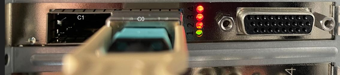
Both connectors support CoF (CXP over Fiber) and data forwarding protocols. Each fiber connector has its own LEDs: Four LEDs are assigned to connector C0, and one LED is assigned to connector C1.
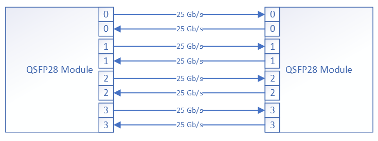
Each connector supports QSFP28 optical modules. A QSFP28 interface provides 4 fiber connections in both directions, i.e. 4 RX and 4 TX connections. A fiber connection is referred to as lane in the operator documentation. Each QSFP28 port has 4 fiber lanes in both RX and TX direction, labeled 0 to 3. Each lane operates at 25 Gbit/s. Thus, a single QSFP28 connector can transport 100 Gbit/s accumulated bandwidth in TX and RX direction.
imaFlex 2 Dual 100 offers data forwarding capabilities to transmit data bidirectionally across multiple frame grabbers. Data forwarding in VisualApplets supports various topologies to transport data and metadata, including daisy-chain and more advanced models. Data forwarding behavior is fully controlled by the user through VisualApplets operators. Camera data, applet‑generated data, and metadata can be transmitted independently in both TX and RX directions. VisualApplets also multiplexes lanes, allowing metadata and regular image data to be sent simultaneously over a single fiber lane using two separate virtual channels. Metadata is prioritized to ensure timely delivery.
Because fiber technology supports bidirectional communication, an advanced master–slave application can allow the master to control which data slave devices receive and to collect processing results from them. Processed results generated on a slave GPU or CPU can be transferred back via DmaFromPC and then forwarded through data forwarding data operators, back to the master frame grabber.
In a typical data forwarding daisy-chain configuration, selected camera data is forwarded to multiple frame grabbers. These frame grabbers then transmit the data to an external GPU over PCIe with very low latency.
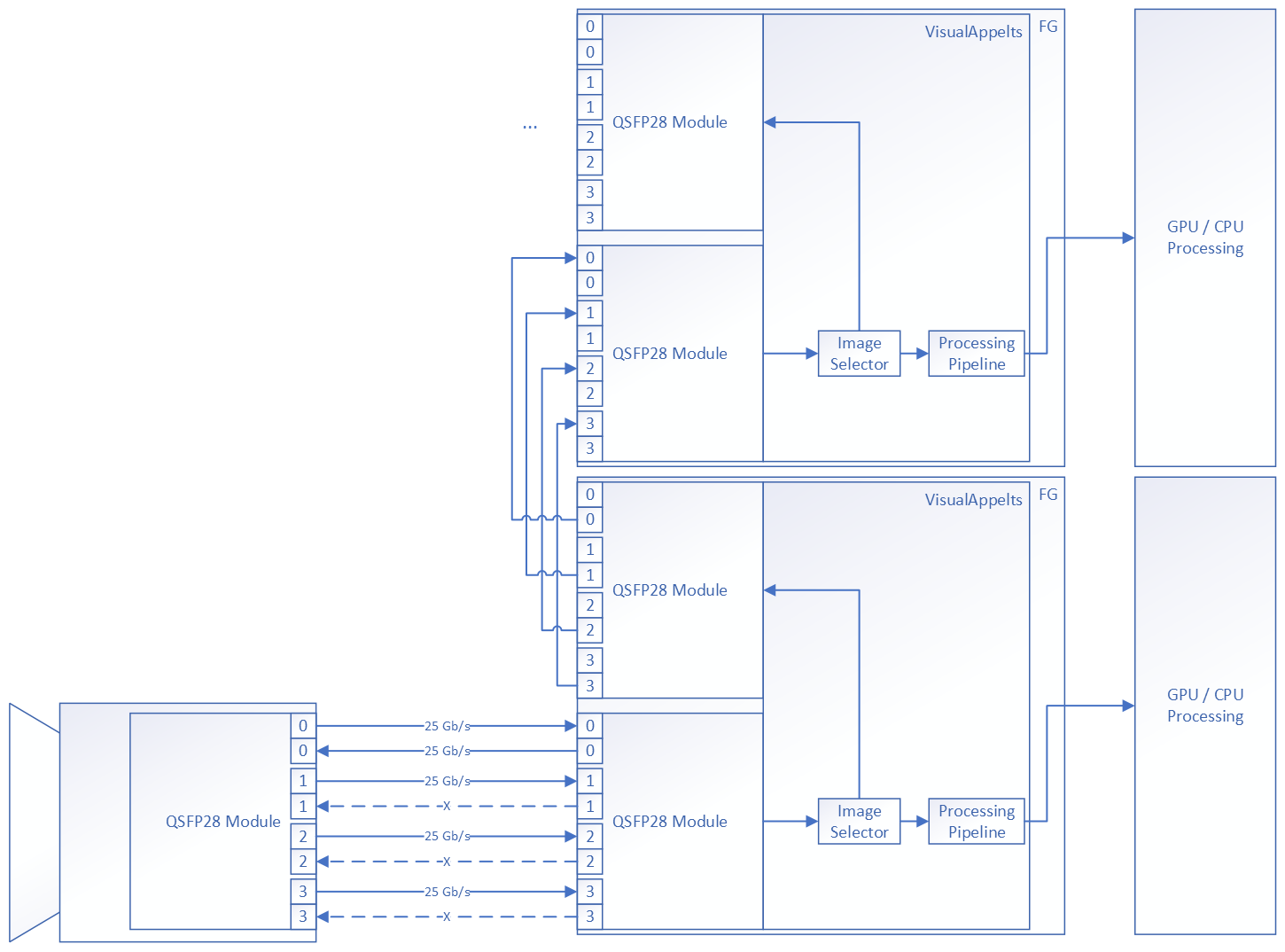
CoF (CXP over Fiber) uses four downstream connections and one upstream connection. Data forwarding links between two frame grabbers are configured to transmit only the required data; they do not transport native CoF traffic but instead carry VisualApplets data and metadata streams. Both CoF and data forwarding are protected by forward error correction (FEC).
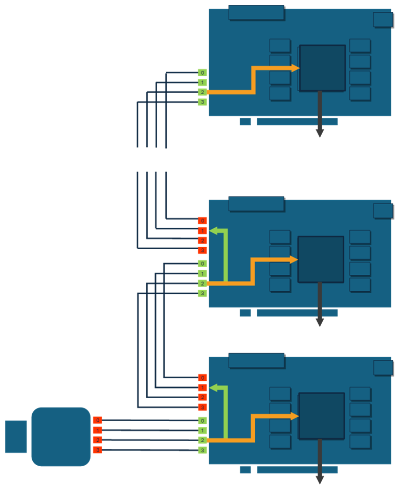
The master frame grabber connects to the camera and forwards the selected data parts to the next slave frame grabber. Each slave frame grabber extracts the data it needs for its own processing and forwards the remaining, unprocessed parts of the image stream to the next slave in the sequence. The last frame grabber in the chain acts as an endpoint and does not forward any data further.
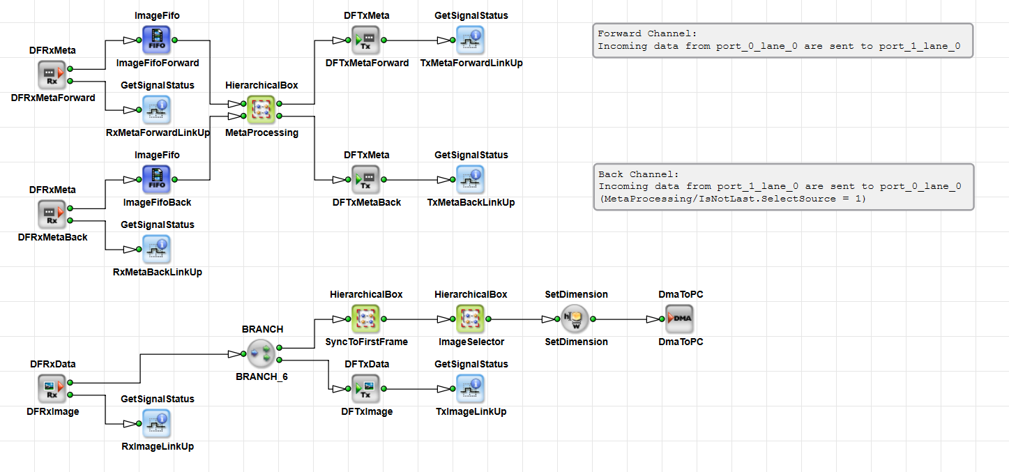
The example above is a simplified representation of a daisy-chain topology. In more advanced configurations, two connected frame grabbers can exchange data freely: they can span 1-, 2-, 3-, or 4-lane connections between each other. RX and TX directions may use different numbers of lanes.
Multiple optical lanes can be combined into virtual channels, allowing several data channels to be transmitted over a single QSFP28 connector. In addition to image data transmission, VisualApplets provides a dedicated meta channel for each optical lane. This meta channel has priority over normal image data and is transmitted with very low jitter and latency, enabling applications to implement time stamping and board-to-board synchronization. Small side-band information can also be transmitted via the meta channel, for example to configure the slave partner on the opposite end of the fiber connection. The partner can return control and status information over its own meta channel back to the master. Each frame grabber can also send processed image data to its partner at an aggregated bandwidth of up to 100 Gb/s.
Up to four meta channels can be spanned between two frame grabbers over a single QSFP28 interface, independently in TX and RX directions. Each meta channel operates at 25 Gb/s. Image-data channels can span 1, 2, 3, or 4 optical lanes to form a virtual data-transmission channel.
A QSFP28 data forwarding interface allows the following combinations of virtual data channels:
-
1 x4 channels: 100 Gbit/s
-
1 x3 channels running at 75 Gbit/s and 1 x1 channel running at 25 Gbit/s
-
2 x2 channels running at 50 Gbit/s each
-
1 x2 channels running at 50 Gbit/s and 2 x1 channels running at 25 Gbit/s
-
4 x1 channels running at 25 Gbit/s each
The RX and TX sides operate completely independently. This means that the backward (RX) direction can be implemented or omitted as needed. If it is implemented, it does not have to be symmetrical to the forward (TX) direction.
Meta channels and data channels operate independently. Each meta channel uses exactly one fiber lane and runs at 25 Gb/s. Meta channels are designed for transmitting small amounts of data. Because they have priority, a meta‑channel transmission temporarily pauses regular data transmission on the same fiber lane.
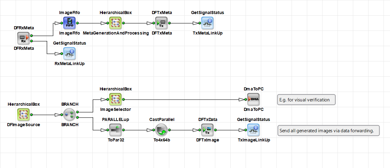
To support data forwarding functionality, VisualApplets provides the following operators:
-
DFTxData – operator for transmitting image data, spanning 1–4 lanes.
-
DFRxData – operator for receiving image data, spanning 1–4 lanes.
-
DFTxMeta – operator for transmitting metadata, 1 lane.
-
DFRxMeta – operator for receiving metadata, 1 lane.
-
DFLed – operator for accessing the front-slot QSFP28 LEDs (bicolor: red, green, orange). C1 has 1 LED; C0 has 4 bicolor LEDs (one per lane).
Basler provides data forwarding examples as a VisualApplets design, along with a C++
SDK control application. In these examples you can see how to use these operators for
data forwarding. The examples are available as VisualApplets examples at Examples/Acquisition/DataForwarding. You find documentation for these data forwarding examples in the 'Data Forwarding for CoaXPress over Fiber Frame Grabber' topic in the tutorial.
Under certain restrictions, more complex camera–frame grabber models are possible. The optical transmission between two frame grabbers has extremely low latency: approximately 120 ns for a data word to travel from one frame grabber to another.
A daisy‑chain topology is the most common approach for distributing processing loads across multiple CPU/GPU clusters:
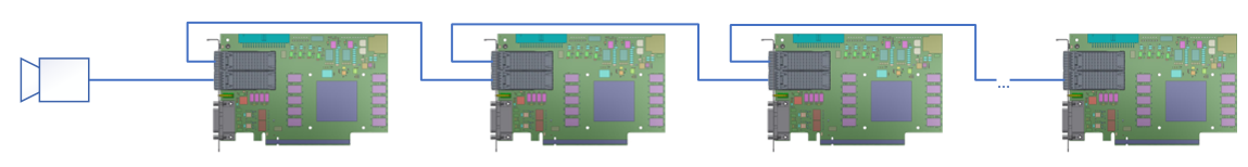
The master frame grabber connects to the camera; the second QSFP28 port connects to the next slave. Each slave processes part of the incoming data and forwards the remaining data to the next device. The last frame grabber in the chain serves as the endpoint. All frame grabbers except the last use both QSFP28 ports.
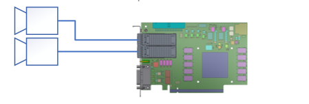
For some applications, it is possible to connect two 100‑Gb/s cameras to a single frame grabber. This requires that the cameras are not operating at their maximum bandwidth, or that pre‑processing in VisualApplets can be performed before storing the data in RAM to slightly reduce the bandwidth so both camera streams fit into the two RAM interfaces. In this configuration, the frame grabber must perform additional processing in VisualApplets to reduce the resulting data rate so it matches the limited PCIe throughput of approximately 13 GB/s.
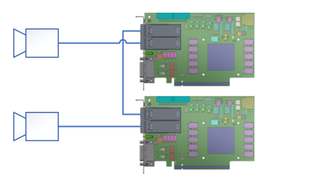
In this case, each frame grabber connects to its own camera. The second QSFP28 port is used for inter‑frame‑grabber communication, enabling data exchange at up to 100 Gbit/s in both directions for complex computing tasks and synchronization.
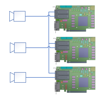
In this topology, each frame grabber connects to its own dedicated camera. The central frame grabber uses its remaining QSFP28 port to connect to two other master frame grabbers via a special fiber cable that splits four lanes into two QSFP28 modules with two lanes each. The only direct connections for the two outer frame grabbers are the full four‑lane links to their respective cameras and the two‑lane links to the central frame grabber. These two lanes enable communication between the frame grabbers at speeds of up to 50 Gbit/s.
