Most VisualApplets applications require the acquisition of camera images, process the image through image processing algorithms and output the results to the host PC. Besides that users want to monitor the original monitoring images. Thus we need two image outputs. The original monitoring images and the processed results of the algorithmic implementation. In the following we will implement a VisualApplets design which fulfills the following specification:
- grayscale images using a Camera Link camera in base configuration mode
- maximum resolution = 1024 x 1024 pixel @ 8Bit/pixel
- buffer images and forward every 10th acquired image to the host PC (monitoring)
- binarize each of the acquired images uising thresholding and output the resulting images to the host PC
- the binarized output images have to be in the format: 0 = black, white = 255 (8Bit/Pixel)
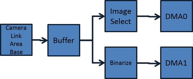
Using the specification, we can generate a block diagram.
As we can see images are grabbed and buffered. After the buffer the processing pipeline is split into two paths. The first path is responsible for the output of every 10th image for monitoring. The second path includes the binarization and the output of the binary images.
Most VisualApplets implementations follow the same principle: Image acquisition and buffering comes first. After the buffering, the image processing logic is located. In 'Data Flow ' you can find more information on VisualApplets processing pipelines and the basic setup of designs. In the following we will go through the implementation of a VisualApplets design which fulfills the specification step by step. Besides the VisualApplets implementation, we will verify the design using the build-in simulation and use the design in real hardware.
-
We will start with the basic operators we used in the previous examples. These are the camera operator CameraGrayAreaBase, the buffer ImageBuffer and the operator to transfer the results to the host PC, namely DmaToPC. In contrast, this time we will need a second DmaToPC module in the design to transfer the original image as well as the binarized results. Locate and rename all operators as shown in the following design.

-
As you can see, we renamed the DMA modules to DMA0_OriginalImages and DMA1_BinarizedImages. Thus we gave them an index. That's because each DMA channel uses a channel index. This channel index is used to access the data from any PC software. Most non FPGA-internal resources use an index to specify their location. Some of the operators using FPGA external hardware are the camera operators, operators using DRAM e.g. the ImageBuffer, operators using general purpose input outputs e.g. trigger signals and DMA operators. In fact, all operators which are in our design so far are using external resources and can be allocated to an index. The camera operator can be allocated to the Camera Link port A or B. The buffer can be allocated to one of the four DRAMs on the microEnable IV VD4-CL and the DMA to one of the DMA channels. A detailed explanation of the use of the device resources can be found in 'Allocation of Device Resources'. A list of the available device resources for all supported hardware platforms is presented in Device Resources.
Most of the device resources can be changed using the resource dialog window in VisualApplets. Some can change their resources using the operator's parameters. To change a device resource, we have to open the resource dialog window which can be accessed from → or by using the icon in the edit menu bar.
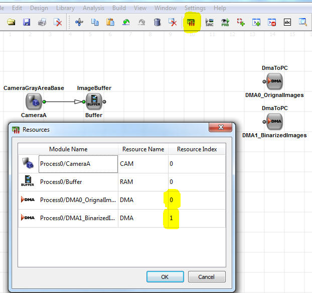
Ensure that the DMA module DMA0_OriginalImages is allocated to index 0 and DMA1_BinarizedImages is allocated to index 1. The camera module should be allocated to index 0 which represents Camera Link port A. We don't really care which of the DRAM chips our buffer is using, so we let VisualApplets choose an index automatically if there is a conflict between some memory operators. In general, VisualApplets will always chose an unused index. If you have two camera modules and delete the module using index 0, the remaining camera module will use index 1. So ensure to check all device resource indices before the start the build of the applet. The resource indices cannot be changed after synthesis.
-
Next, we need to include our image processing algorithms. As we have to implement two different image processing algorithms, we need to branch our pipeline into two paths. This is simply done by a branch operator. Locate the operator in the base operator library and drag it into your design. When you release the mouse button a window will pop-up which will allow users to specify the number of output links i.e. the number of branches. Select two and OK. You will now have a branch module in your design with two output links and one input link. Move the module next to the buffer and connect them.

We now have branched our pipeline and can implement both image processing algorithms between the branch and the DMA modules.
-
First, we will implement the original image output path where only every 10th image is required to be output. Instead of placing all required operators on the main design level, we will use a hierarchical box. With the help of hierarchical modules, it is practical to implement a hierarchical structure into your design and combine an arbitrary number of operators to a new operator. The use of hierarchical modules ease the overview of the construction area. Insert an hierarchical box with one input and one output into your design. You can find the hierarchical box in the base operator library, from the design area pop-up menu or form the main menu "Design".
Place the HierarchicalBox module between the branch and the DMA and connect them. You can rename the module using it's context menu or by selecting it and hitting the F2 key.

To edit the hierarchical module content just double-click on it. A new blank design window will open. It only includes the input and output connectors. We will place the required operators in-between and connect them to the ports. To exit the hierarchical module hit Backspace or icon
 .
.
To remove 9 out of 10 images, we need the operators as shown in the following.

and parameterization:
-
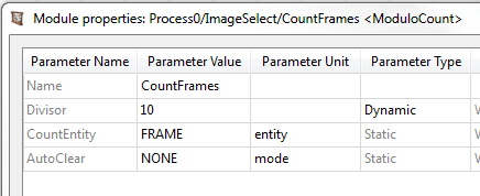
Properties of module CountFrames
-
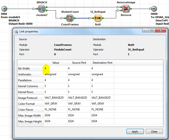
Link Properties of the output of module CountFrames
-
Properties of module Not0
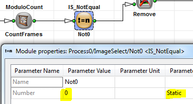
How it works: The CountFrames module will replace the pixels of each image by a value between 0 and 9. Hence, it will repetively count from 0 to 9 with each image. Module Not0 will replace every pixel of each image by value 1, if the current count value is not 0. The RemoveImage module deletes each image, if the pixel value of the second input "Rem" is value 1. Thus, image number 0, 10, 20, 30, ... will be bypassed. All other images will be deleted.
-
-
For the implementation of the binarization we will add another hierarchical module into the design.

The operators in this hierarchical module are "Is_GreaterThan" and "Scale".

Module ThresholdFrom represents the actual binarization. For each input pixel value grater than value specified by parameter Number, value one is output, otherwise zero. Thus, the output bit depth of the module will be one bit. You can check this by opening the link properties. As we do not want to output one bit values, we need to bring our results to eight bit values. A very simple solution to do is to scale each of the values with 255. Thus, binary value one becomes 255 and binary value 0 remains at 0. Set the parameters of the ScaleBy255 module to the following values.
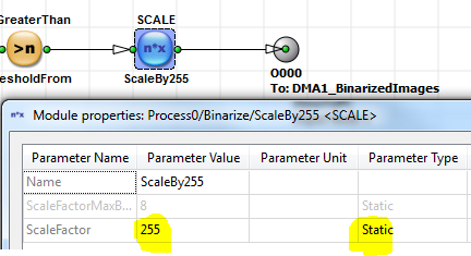
As you can see, we have set the parameter type of parameter ScaleFactor to Static. For this operator this is very important as it will require much less FPGA resources compared to a dynamic parameter. In general, always set parameters to a static type if you know that you will not need to change them after synthesis.
-
- The final step of your implementation will be the check for design rule errors. Perform a DRC to check for errors. If you have no errors you can now build your design and use it in hardware. In alternative, you can verify your implementation using the simulation which is shown in the next section. Do not forget to save your design from time to time.
For most designs it is very useful to verify the functionality of the implementation using the simulation before the use in real FPGA hardware. We will verify our design using the simulation in the following.
-
Preparation
First we will need an image to simulate. You will need to use an image file in TIFF or BMP format. You have to use an image with a single color component if you like to inject the image data to an image processing pipeline using grayscale images as in our example. More information about allowed image files for simulation can be found in 'Simulation'. There are some sample images in the VisualApplets installation folder.
-
Sources and Probes
Image files can be injected to any image transporting link using "simulation_source"" modules and can be monitored on any other link using "simulation_probe" modules. In our example, we add a simulation source to the link between the camera and the buffer and simulation probes according to the following screenshot. You can add simulation sources and probes from the "Analysis" menu, from the context menu of the design window, or simply from the icons marked in the Figure.
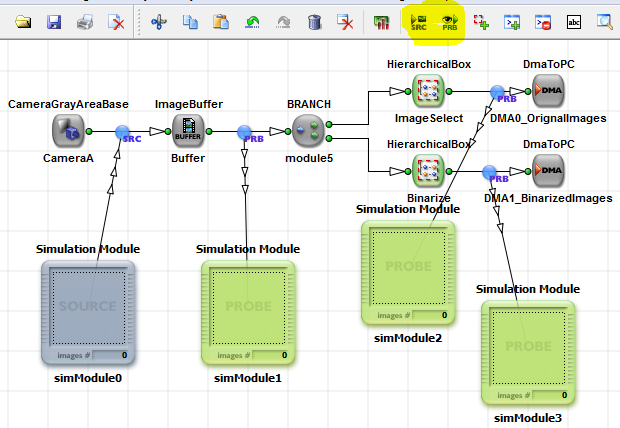
-
Add Image File
To add an image file to the simulation source, open the Simulation Source Viewer using a double-click on the source in your design. Now simply drag-and drop your image file to the Simulation Source Viewer window or use the → menu.
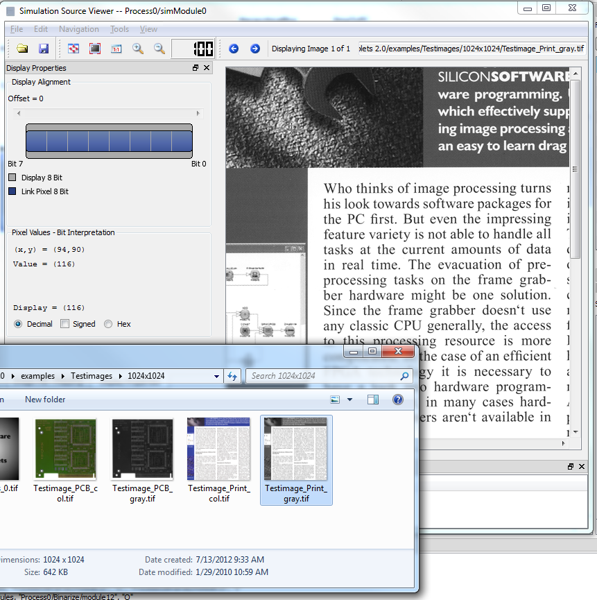
The image file was now added to the simulation source. You can add more files to the source by simply dragging them on the module or window. At the bottom of the Simulation Source Viewer Windows you can see all images in the sequence.
-
Simulation Start
We are now ready to start the simulation. Select → ( F9 ) to open the main Simulation window. Each time you open this window a design rules check will automatically be performed. It is not possible to simulate a design with a failed design rules check.
In VisualApplets, simulations are processed in cycles. Each cycle represents the injection of an image from all simulation sources in the design. Simply click on to start the simulation. VisualApplets will now perform the simulation. Depending on the complexity of the design this might take some seconds.
-
Check Results
We can now check the results of our simulation. Close the Simulation window. The simulation probes should now have been filled with results.
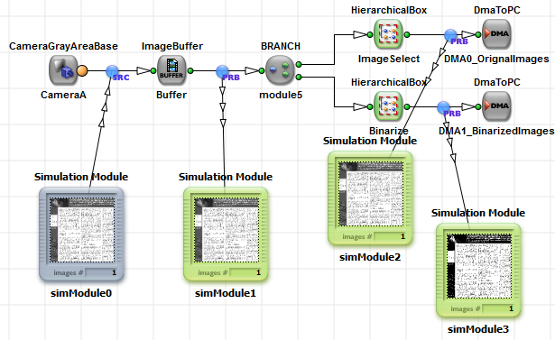
If you open the Simulation Probe Viewer of the probe located behind the binarization, you can immediately see if the simulation worked. The image should include pixels having values 0 and 255.
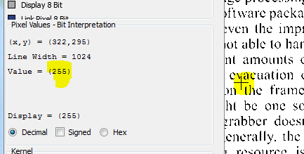
Results can now be saved to disk, if required.
-
Sequence Simulation
We could verify the binarization in the previous step. However, a single simulation image is not sufficient to verify the monitoring output as only every 10th image is supposed to be transfered to the host PC. Thus we need to simulate a sequence of images.
-
Open the Simulation window once again.
-
Click on to reset the sequence from previous simulations. In general, if you want to start a new simulation, it is useful to always reset the simulation to avoid user errors.
-
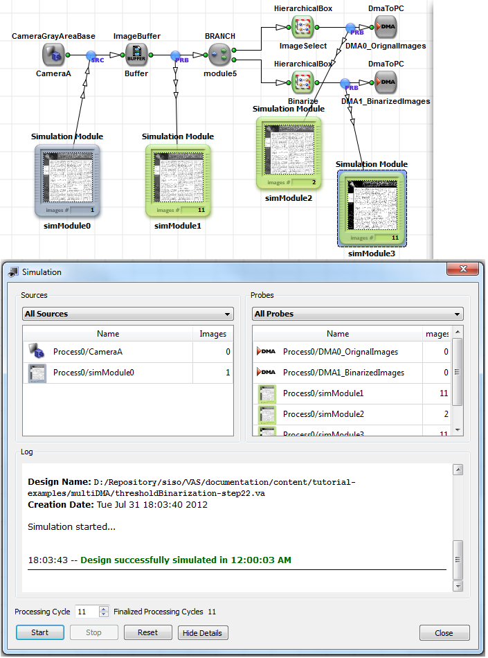
Click on to simulate one image. We will get a result in each of the simulation probes. It is not required to close the Simulation window now. You can get the current number of images in a simulation probe by looking at the numbers of the modules in the design window.
-
Now perform another cycle by a click on . This time, the image number of all simulation probes should have been increased to two except the one at the DMA0 module.
Repeat this step until you have simulated 11 cycles in total. The probe at DMA 0 should now include two images. This shows the correct functionality of our implementation.
-
Instead of clicking 11 times on you can set the number of processing cycles using the spin box in the Simulation window. The simulation result will be the same. Also, you can set 10 simulation cycles, start them and start the next 10 cycles after. As you like...
-
After we verified the functionality of our implementation we can test and use it in hardware. You will need to build your design to get the hardware applet file HAP. (User Manual: 'Build') Ensure that your design matches the hardware platform e.g. mE4VD4-CL in our example. Moreover ensure that your project is using the correct architecture e.g. Windows 64 Bit. It has to be the same as the installed Framegrabber SDK. Start the build by → ( F7 ). VisualApplets will now use the FGPA manufacturer tool to translate your design into the FPGA bitstream.
The result of the synthesis is an HAP-file. It contains the FPGA bitstream and the software interface to access data and parameters. The HAP file is located in your Framegrabber SDK installation directory in subdirectory "Hardware Applets" or, if no Framegrabber SDK is installed or you selected another target runtime, the file is located in the folder specified in the system settings (See 'System Settings').
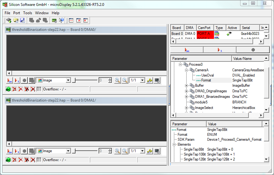
We will test our design in the Framegrabber SDK tool microDisplay. microDisplay is a tool for a first test of applets. Open microDisplay and load the applet. microDisplay will show two DMA image windows, namely the original image window where only every 10th image is shown and the second DMA window showing the binarized images. A detailed explanation on the use of applets in the Framegrabber SDK can be obtained from the Framegrabber SDK documentation.

 Prev
Prev

